Fraunhofer Institut für Angewandte Festkörperphysik IAF
AlScN - alternative material for more efficient smartphone hardware
The ever-growing mobile data transfers in the wake of 5G require the use of more and higher frequency ranges, all of which need to be accommodated within a single mobile device. Thus, the demands on radio frequency (RF) components are constantly increasing. The Fraunhofer Institute for Applied Solid State Physics IAF has developed novel, compact, and energy-efficient high-frequency / high-bandwidth RF filters to meet those needs. During the project "PiTrans" the researchers have managed to grow aluminum scandium nitride (AlScN) with the required industrial specifications and to realize novel electroacoustic devices for smartphones.
The amount of RF components built into a single smartphone has increased significantly over the past years and there is no end in sight. Predicting this trend in 2015, the project " PiTrans - Development of AlScN layers for the next generation piezoelectric RF filters" set out to develop and produce improved RF piezo-transducers with ternary AlN-based nitrides as the piezo-active layer. Within the five years of the project, the researchers succeeded in growing highly crystalline AlScN layers and realizing surface acoustic wave (SAW) resonators that meet the increasing requirements of the industry. For the growth of the material, which is also promising for other power electronic applications, a modern magnetron-sputtering infrastructure was established at Fraunhofer IAF. The project was funded by a "Fraunhofer Attract" excellence stipend program and successfully completed in January 2020 under the leadership of Dr. Agn? Zukauskait?.
Potential and challenges of AlScN
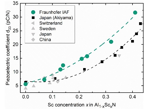
To this day, AlScN remains the most promising new material to replace conventional aluminum nitride (AlN) in RF filter applications inside mobile phones. By introducing scandium (Sc) into AlN, the electromechanical coupling and piezoelectric coefficient of the material is increased, enabling a more efficient mechanical to electric energy conversion. This allows the production of much more efficient RF devices. However, the instability of the piezoelectric AlScN crystal phase has so far been a problem for industrial use of the material, as segregation of wurtzite-type AlN and cubic ScN usually occurs during growth. "Back in 2015, we knew the potential of AlscN, but we needed to find the right conditions to grow it in a stable and scalable process," remembers Dr. Zukauskait?, who led her team to success.
Successful growth and device development
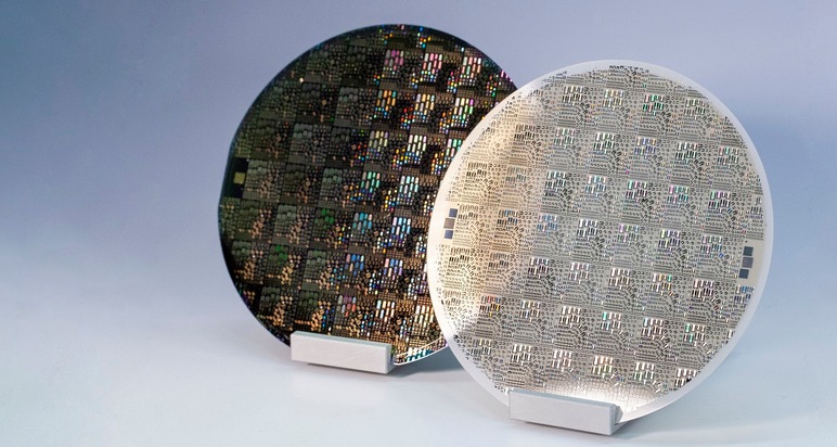
In the course of the project, the scientists at Fraunhofer IAF managed to grow highly crystalline AlScN layers with a wide range of compositions up to a Sc content of 41 percent. A good homogeneity of the layers was achieved across the entire silicon (Si) wafer up to 200 mm in diameter, which meets the requirements of industrial productions. Besides these industry-relevant results, the project team also succeeded in realizing an epitaxial growth on lattice-matched sapphire (Al2O3) substrates through a special magnetron sputter epitaxy (MSE) method of deposition, which will be useful for future material research.
In addition to the successful material development, the researchers produced three generations of test structures to demonstrate the performance of the AlScN thin films. The implementation of MSE to produce AlScN/Al2O3-based resonators lead to an electromechanical coupling increase of up to 10% at 2 GHz frequency. In a collaboration with the companies Evatec and Qualcomm, a non-polar AlScN thin film was also developed that further improves the electromechanical coupling of SAW resonators. This technology is currently being further researched and first results have just recently been published in a scientific paper.
AlScN for other applications
"We see AlScN as a very promising candidate for enabling future applications that capitalize on the piezoelectric effect, such as sensor technologies and high electron mobility transistors," explains Dr. Zukauskait?. The success of the project "PiTrans" led to the acquisition of two further projects involving AlScN technology at Fraunhofer IAF. In the project "mAgnes", wide-band current sensors such as those used in e-cars are being researched; and in the project "SALSA", the research team is developing new types of switchable high electron mobility transistors (HEMTs). Both projects benefit from the developed expertise in AlScN growth and AlScN-based device development as well as the necessary infrastructure established at Fraunhofer IAF.
------------------------------------------------------------------------------------------------------
About Fraunhofer IAF
The Fraunhofer Institute for Applied Solid State Physics IAF ranks among the leading research institutions in the field of compound semiconductors. Based on these semiconductors, IAF develops electronic and optoelectronic components as well as integrated circuits and systems. In a clean room of 1000 m² and additional laboratory space covering 3000 m2, epitaxy and processing equipment along with measurement technologies are available to realize high frequency circuits for communication technology, voltage converter modules for electrical engineering, infrared and UV detectors for safety and security applications, as well as infrared laser systems for medical technology. Important innovations of the institute include high brightness white light-emitting diodes for lighting technology, energy-efficient power amplifiers for mobile communications and highly sensitive laser systems for real-time spectroscopy.
Fraunhofer Institute for Applied Solid State Physics IAF
Tullastraße 72 | 79108 Freiburg | Germany
+49 761 5159-418
www.iaf.fraunhofer.de/en

